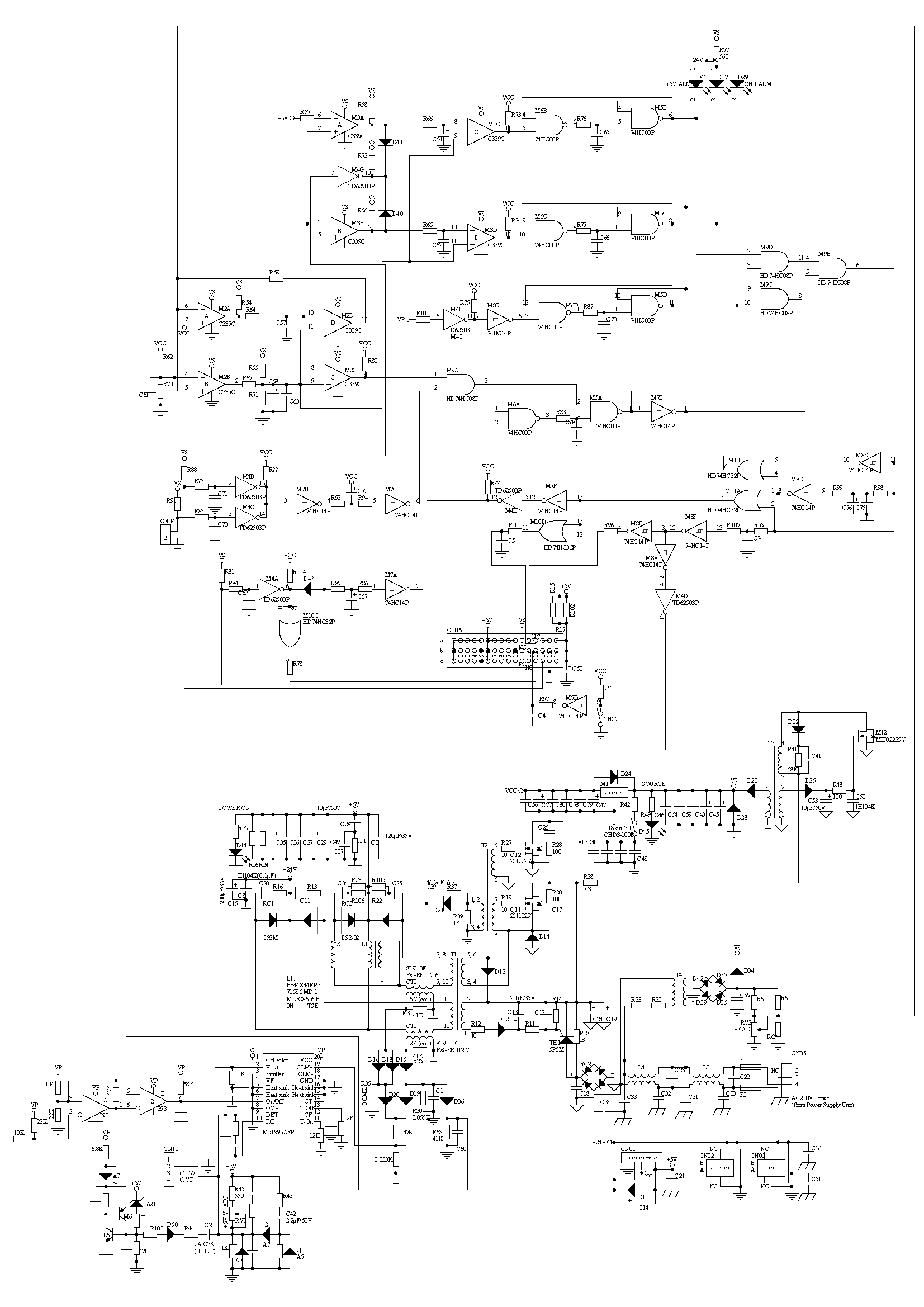
The control power supply unit (as shown in the figure) provides +5V and +24V DC power supply for I/O unit, power on unit and programming box through CN01, CN02 and CN03 sockets. The remote switch control function is provided through its CN04 socket. It through CN06 provides +5V power supply, status signals for system control board and receives control signals. Rated input voltage: 200/220VAC, allowable fluctuation range: -15%-+10% (170-242VAC), frequency: 50/60Hz±2Hz (48-62Hz). The output voltage is +5VDC/10A, +24VDC/4.0A. There are two green LED indicators, SOURCE and POWER ON, respectively indicating that the AC power input is normal and the DC power normal. Three red LEDs +5V, +24V and OHT respectively indicate +5V over-current or over-voltage alarm, +24V over-current alarm and internal power output silicon rectifier overheating alarm. In addition, when the temperature in the module reaches 65℃, pulse signal is sent to the system control board.
The circuit is mainly divided into three parts: auxiliary power supply, main power supply and fault detection circuit.
Auxiliary power supply
AC200/220V is input from CN05 socket. After rectification and filtering, it outputs about 310VDC voltage from full bridge RC2 to supply power to NMOS FETs M12 and Q11. Another AC branch is through transformer T4, diode full bridge, capacitor C55, etc. to generate about 5V reference voltage on resistor R69, which is sent to the fault detection circuit.
The self-excited oscillation circuit is composed of M12, 3-4, 1-2 coils of transformer T3, D25, C53, R48 and C50. Through 6-7 coil of T3, D23, D28 and filter capacitors, about 23VDC power supply voltage VS is obtained, and the SOURCE indicator is turned on. The power supply voltage gets VP power supply through thermal switch OHD3-100B, which supplies power to PWM control chip M51995AFP and comparator chip 393. Once the components RC3 and RC1 of +5V and +24V output circuit overheat, VP will be cut off. In addition, the +5V VCC power supply is obtained from the VS through a 3-terminal voltage regulator M1 to supply the fault detection circuit.
Main power supply
The +5V/10A and +24V/4.0A are respectively obtained from the secondary side of transformer T1 of main oscillation circuit through silicon diodes RC3, RC1 and capacitors. The frequency of oscillation pulse generated by PWM control chip M51995AFP is determined by the resistors and capacitors connected to its pins 11-13, which is about 189kHz. The feedback signal is provided by the voltage dividing circuit composed of R45, RV1 and other components, connected to the DET end, and through the resistor-capacitor circuit connected to the F/B end, and the voltage at DET is about 2.5V. The output Vout is applied to the grids of Q12 and Q11 through transformer T2, and coupled to the main power output side through (3,4-5,6) coils of transformer T1. At the same time, from the (1-2) coil of T1 the induced pulse signal is rectified and filtered and applied to the thyristor TH1 to make the resistor R18 nearly short-circuit.
The current inductors CT2 and CT1 detect the current changes in the output circuits of +5V and +24V main power supply respectively, and input them to the CLM+ end of M51995AFP through diodes and resistors, etc., so as to realize the so-called “pulse by pulse current limiting”. In addition, the +24V over-current signal is taken out from the resistor R68 and sent to the fault detection circuit.
Fault detection circuit
The +5V main power over-current detection circuit is composed of voltage comparators M3A, M3C and NAND gates M6B, M5B, etc. In case of over-current, M3A outputs high level, M3C and M5B output low level, and the +5V alarm light is on.
The +5V overvoltage detection circuit is composed of 6V voltage regulator 621, triodes L6 and M6, etc. When overvoltage occurs, 621 turns on, L6 and M6 turn on, the reverse input end of voltage comparator 393B turns to low level, the On/Off end of M51995AFP turns to high level, the chip stops oscillation, +5V turns to 0, and the +5V alarm light is also turned on.
The +24V overcurrent detection circuit is mainly composed of voltage comparators M3B, M3D and NAND gates M6C, M5C, etc. When the +24V main power supply is overcurrent, the signal taken out from the R68 makes the output of M3B become high level, and then causes the output of M5C to be low level, and the +24V alarm light is turned on.
The overheat detection circuit of main power supply is composed of thermal switch OHD3-100B, buffers M4F, M8C and NAND gates M6D, M5D, etc. When overheat occurs, the thermal switch will be disconnected and VP will be disconnected too. This will make the output of M5D low, and the overheat indicator OHT on.
Through a series of gate circuits such as M9D, M9C and M9B, resistors and capacitors, alarm signals make the reverse input of voltage comparator 393A into a high level, so that the On/Off end of M51995AFP becomes high and the chip stops.
The circuit composed of M9A, M6A, M5A and M7E, etc. is used to detect remote control signal, system control signal, etc. When the power supply is overhauled separately, the pin 1 of CN04 and the 14c and 14b pins of CN06 should be short circuited to signal ground to make the output of M7E high level and ensure the normal operation of each detection circuit.
The system control board receives various status signals of the power module through CN06, including the temperature switch signal in the module sensed by the thermal switch THS2.
Repair cases
Ex. 1 The SOURCE and +5V indicator lights were on when the power was turned on separately (the same below).
This shows that the auxiliary power supply VS was normal, but the +5V main power supply had overvoltage or overcurrent alarm. Whether it was overvoltage or overcurrent, the +5V power supply disappeared, and previous voltage value of each point could not be measured anymore. It seems difficult to judge which situation made the alarm light on. First checked whether the working conditions of M51995AFP were met. Measured the supply voltage of pin 20 or VCC end, that is VP, 46V. The recommended working voltage of the chip is 12-36V. It can be seen that although the SOURCE light was on, the VS was still too high. Checked the components of the self-excited oscillation circuit with a multimeter and found that the capacitor C53 had changed from 10μF to 0.135μF. Replaced it with a 47μF capacitor on hand, the VP dropped to 23V, and the whole power supply returned to normal.
Ex. 2 After power on, SOURCE and POWER ON lighted up normally, but after a period of time, POWER ON went out and +5V alarm light lighted up. The power on time of each test was different, which was irregular from a few seconds to a few hours.
From the phenomenon, it should be caused by the poor contact of the main power circuit. Careful inspection of the main circuit components showed no obvious poor contact or copper foil lead fracture. The power supply VP of M51995AFP was also normal and stable. When the oscilloscope was used to observe the waveform of the relevant pins, the tiny claw of the lead-out measuring clip picked up a pin. It turned out to be that the pin of M51995AFP was poor soldered. But because it was a SMD and small, it appeared OK while measured with a multimeter. Soldered and checked these pins again, the poor contact disappeared.
Ex. 3 After power on, only SOURCE light was on.
POWER ON is not on, indicating that the main power supply is not normal. However, if the main power supply is abnormal, +5V alarm light should be on, unless the output of buffer M7E is low level and the output of NAND gate M5B is locked to high level. The output of M7E was measured, 1.2V, which was really low level. The voltage (potential) of the pins 1, 2 and 3 of the front NAND gate M5A were 4.9V, 4.9V and 4V respectively, which obviously did not conform to the logic relationship of NAND gate. After replacing the four NAND gate chip M5, still only one light was on, and the voltage of pins 1, 2 and 3 became 0V, 3.3-4.8V (unstable) and 4.9V respectively. Continued to check the voltage of each point from back to front while considering the logical relationship. It was found finally that the short wire between 14b and 14c of CN06 socket (convenient for offline maintenance) have been disconnected or touched other solder joint. After solving the problem, the power supply became normal.
Reference
[1] YASNAC XRC Instructions for European Standard, Manual No. RE-CTO-A205, Yaskawa
[2] Datasheet: M51995AP/AFP Switching Regulator Control, REJ03D0835-0300, Rev.3.00, Jun 06, 2008, Renesas